Categories: Automated Wafer Measurement System, Semiconductor, Semiconductor Advanced Metrology System (AMS Series), Wafer Roughness Measuring, Wafer Thickness & Roughness Measuring
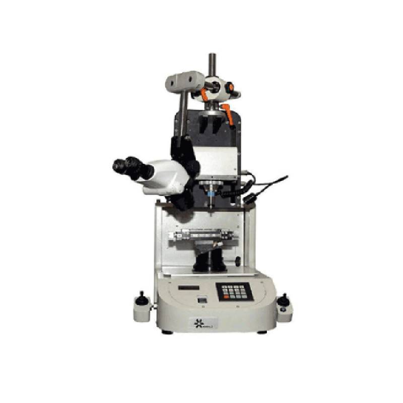
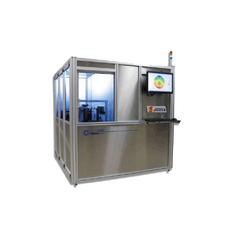
The MPT1000 is Chapman Instruments’ latest non-contact system, providing wafer thickness measurements. It can be used as a production tool for in-line quality inspection, a research and development tool for establishing standards, and compiling data for enhancing productivity. The MPT1000 utilizes a sophisticated non-contact measurement technology with a focused laser spot on the wafer surfaces. Users can measure structured taped wafers after backgrind or dicing. The powerful, user-friendly, Windows® based operational software can be programmed to provide automated wafer thickness maps, execute a series of measurements, or report the data offline for further analysis.
Key Features
- Non-contact, providing non-destructive thickness measurements
- 0.1 μm thickness resolution, providing thickness uniformity and Q/C control
- 1 μm laser spot size on both top and bottom wafer surfaces, providing the ability to distinguish between small features, eg wafers
- Optical Measurement System, providing accurate wafer thickness measurements independent of material properties, especially useful for patterned wafers, GaAs and other wafer types, and dicing
- Wafer Bow and Warp measurements.
Specifications
- Thickness resolution (0.1um) providing uniform TTV for production control of wafers.
- Measurements after back grind or dicing provide flexibility for thickness uniformity control.
- Small focused laser spot (1 um) provides the resolution required for measuring bumped wafers and via features.